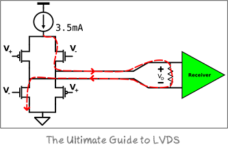
LVDS PCB Layout Guidelines – Expert Tips for Clean Designs! Some lvds pcb layout guidelines for ensuring signal integrity
If you are looking for Some LVDS PCB Layout Guidelines For Ensuring Signal, 40% OFF you've visit to the right place. We have 25 Pics about Some LVDS PCB Layout Guidelines For Ensuring Signal, 40% OFF like Practical Guidelines for High-Speed PCB Layout and Critical Component, PCB Layout Optimisation | PDF | Electrostatic Discharge | Printed and also PCB Design Tips | PDF | Electromagnetic Interference | Printed Circuit. Here you go:
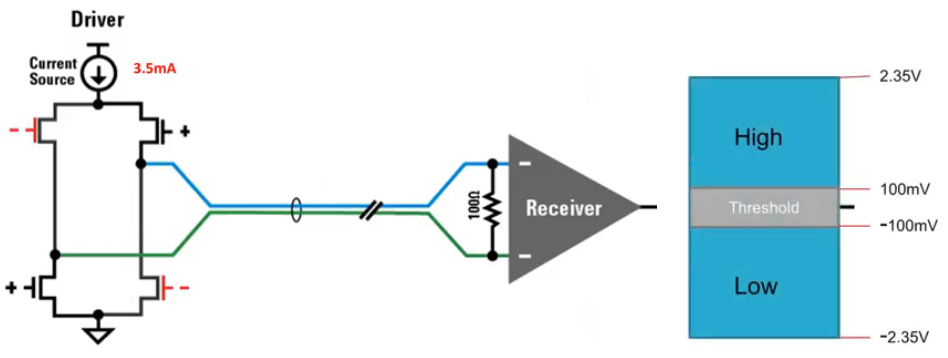
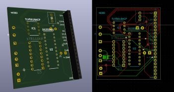
Some LVDS PCB Layout Guidelines For Ensuring Signal, 40% OFF
 www.oceanproperty.co.th
Some LVDS PCB Layout Guidelines For Ensuring Signal, 40% OFF
PCB Layout Checklist - Voler Systems
 www.volersystems.com
PCB Layout Checklist - Voler Systems
How To Design PCB Layout? - Guidelines, Advantages And Disadvantages
 compuinfohub.blogspot.com
How to Design PCB Layout? - Guidelines, Advantages and Disadvantages ...
PCB Layout Design - RaceEL Systems
 www.raceelsystems.com
PCB Layout Design - RaceEL Systems
A Detailed Guide To PCB Layout Design - IBE Electronics
 www.pcbaaa.com
A detailed guide to PCB layout design - IBE Electronics
Top Tips For Successful PCB Layout Design: Guidelines And Best Practices
Top Tips for Successful PCB Layout Design: Guidelines and Best Practices
Top 10 Tips For Efficient PCB Layout Design | 911EDA
 www.911eda.com
Top 10 Tips for Efficient PCB Layout Design | 911EDA
Layout PCB Inverter: Tips And Best Practices For Successful Design
 hillmancurtis.com
Layout PCB Inverter: Tips and Best Practices for Successful Design ...
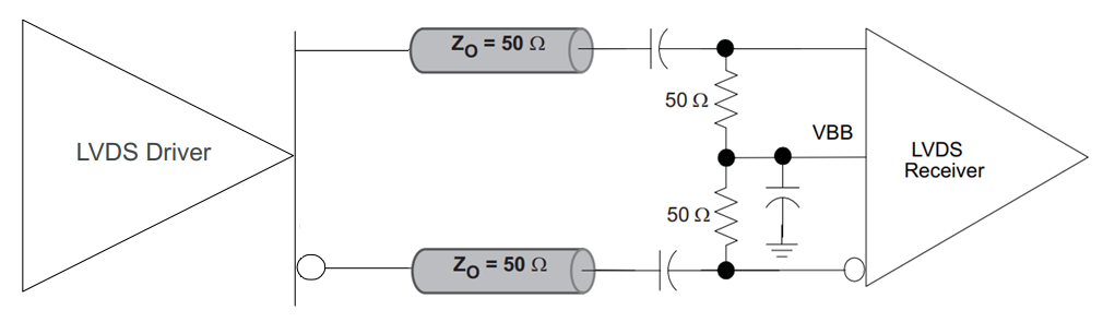
Some LVDS PCB Layout Guidelines For Ensuring Signal Integrity | PCB
 resources.altium.com
Some LVDS PCB Layout Guidelines for Ensuring Signal Integrity | PCB ...
How To Perform PCB Design Review And Layout Clean-Up – PCB HERO
 www.pcb-hero.com
How to Perform PCB Design Review and Layout Clean-Up – PCB HERO
PCB Layout Design By Siemens | PADS Professional | Cadlog
 www.cadlog.com
PCB Layout Design by Siemens | PADS Professional | Cadlog
Complete Guide To PCB Layout Design: Tips, Basics, & Guidelines
 sfxpcb.com
Complete Guide to PCB Layout Design: Tips, Basics, & Guidelines
Practical Guidelines For High-Speed PCB Layout And Critical Component
 www.scribd.com
Practical Guidelines for High-Speed PCB Layout and Critical Component ...
Complete Guide To PCB Layout Design: Tips, Basics, & Guidelines
 sfxpcb.com
Complete Guide to PCB Layout Design: Tips, Basics, & Guidelines
Best Practices In PCB Design | PDF | Printed Circuit Board | Computer
 www.scribd.com
Best Practices in PCB Design | PDF | Printed Circuit Board | Computer ...
Some LVDS PCB Layout Guidelines For Ensuring Signal Integrity | PCB
Some LVDS PCB Layout Guidelines for Ensuring Signal Integrity | PCB ...
PCB Layout Guidelines | Design Rules & Requirements | Tips
 www.wellpcb.com
PCB Layout Guidelines | Design Rules & Requirements | Tips
Pcb Layout Guidelines For Design By PCBCART - Issuu
 issuu.com
Pcb layout guidelines for design by PCBCART - Issuu
Practical PCB Design Layout Rules - Leading PCB Manufacturer - Arisentec®
 arisentecpcb.com
Practical PCB design layout rules - Leading PCB Manufacturer - Arisentec®
Some LVDS PCB Layout Guidelines For Ensuring Signal Integrity | PCB
 resources.altium.com
Some LVDS PCB Layout Guidelines for Ensuring Signal Integrity | PCB ...
PCB Design Tips | PDF | Electromagnetic Interference | Printed Circuit
 www.scribd.com
PCB Design Tips | PDF | Electromagnetic Interference | Printed Circuit ...
BASIC PCB Design Rules – Layout
 epci.eu
BASIC PCB Design Rules – Layout
Some LVDS PCB Layout Guidelines For Ensuring Signal, 40% OFF
 www.oceanproperty.co.th
Some LVDS PCB Layout Guidelines For Ensuring Signal, 40% OFF
PCB Layout Optimisation | PDF | Electrostatic Discharge | Printed
 www.scribd.com
PCB Layout Optimisation | PDF | Electrostatic Discharge | Printed ...
Expert PCB Layout Service For Optimal Designs - PCB Layout Services And
 zinponpcb.en.made-in-china.com
Expert PCB Layout Service for Optimal Designs - PCB Layout Services and ...
How to perform pcb design review and layout clean-up – pcb hero. Some lvds pcb layout guidelines for ensuring signal integrity. Some lvds pcb layout guidelines for ensuring signal integrity