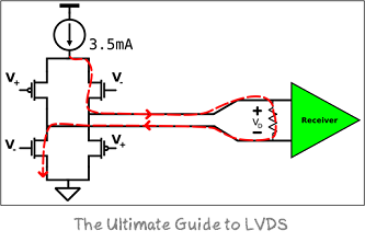
LVDS PCB Layout Guidelines: Optimize Your Design! High current pcb design guidelines
If you are looking for PCB Layout Guidelines for USB Type-C you've came to the right web. We have 25 Images about PCB Layout Guidelines for USB Type-C like Some LVDS PCB Layout Guidelines For Ensuring Signal, 40% OFF, Some LVDS PCB Layout Guidelines For Ensuring Signal, 40% OFF and also PCB Design Layout Guidelines for Engineers | Advanced PCB Design Blog. Read more:
PCB Layout Guidelines For USB Type-C
PCB Layout Guidelines for USB Type-C
PCB Layout Guidelines And Considerations
 www.microcontrollertips.com
PCB layout guidelines and considerations
PCB Design Layout Guidelines For Engineers | Advanced PCB Design Blog
 resources.pcb.cadence.com
PCB Design Layout Guidelines for Engineers | Advanced PCB Design Blog ...
LVDS Board Design Guidelines: Altera FPGAs & PCB Layout
 studylib.net
studylib.net
LVDS Board Design Guidelines: Altera FPGAs & PCB Layout
Some LVDS PCB Layout Guidelines For Ensuring Signal Integrity | PCB
 resources.altium.com
Some LVDS PCB Layout Guidelines for Ensuring Signal Integrity | PCB ...
Pcb Layout Design Priority 1 Design Pcb Layout Design And Manufacture
 electricalcircuit.z6.web.core.windows.net
pcb layout design Priority 1 design pcb layout design and manufacture
Pcb Layout Guidelines Top 5 Pcb Design Rules You Need To Know
 electricalcircuit.z6.web.core.windows.net
pcb layout guidelines Top 5 pcb design rules you need to know
Component Placement In PCB Design & Assembly | Sierra Circuits
 www.protoexpress.com
Component Placement in PCB Design & Assembly | Sierra Circuits
Some LVDS PCB Layout Guidelines For Ensuring Signal, 40% OFF
 www.oceanproperty.co.th
Some LVDS PCB Layout Guidelines For Ensuring Signal, 40% OFF
Some LVDS PCB Layout Guidelines For Ensuring Signal Integrity | PCB
Some LVDS PCB Layout Guidelines for Ensuring Signal Integrity | PCB ...
PCB Layout Guidelines For High Speed Applications - HardwareBee
 hardwarebee.com
PCB Layout Guidelines For High Speed Applications - HardwareBee
PCB Layout Guidelines For Decoupling And Bypassing Capacitors
 www.onelectrontech.com
PCB Layout Guidelines for Decoupling and Bypassing Capacitors ...
High Current Pcb Design Guidelines - Design Talk
 design.udlvirtual.edu.pe
High Current Pcb Design Guidelines - Design Talk
Main Design Guidelines & Layout Rules On High Speed PCB
 www.integrasources.com
Main Design Guidelines & Layout Rules on High Speed PCB
Some LVDS PCB Layout Guidelines For Ensuring Signal, 40% OFF
 www.oceanproperty.co.th
Some LVDS PCB Layout Guidelines For Ensuring Signal, 40% OFF
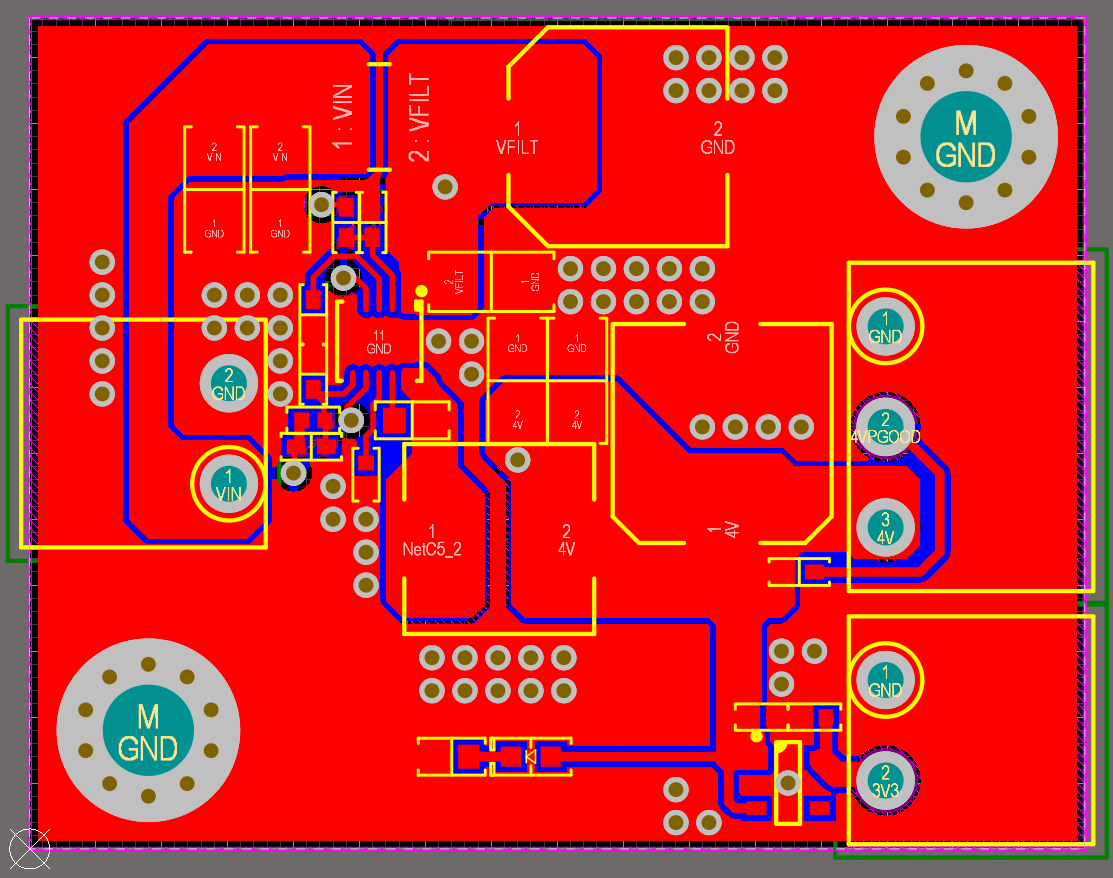
Switched-Mode Power Supply PCB Design Guidelines | Altium
 resources.altium.com
Switched-Mode Power Supply PCB Design Guidelines | Altium
SMPS PCB Layout Guidelines In Altium Designer
 resources.altium.com
SMPS PCB Layout Guidelines in Altium Designer
Pcb Layout Guidelines Can Bus Pcb Circuits – Eroppa
 eroppa.com
Pcb Layout Guidelines Can Bus Pcb Circuits – Eroppa
Some LVDS PCB Layout Guidelines For Ensuring Signal Integrity | PCB
 resources.altium.com
Some LVDS PCB Layout Guidelines for Ensuring Signal Integrity | PCB ...
Some LVDS PCB Layout Guidelines For Ensuring Signal Integrity | PCB
 resources.altium.com
Some LVDS PCB Layout Guidelines for Ensuring Signal Integrity | PCB ...
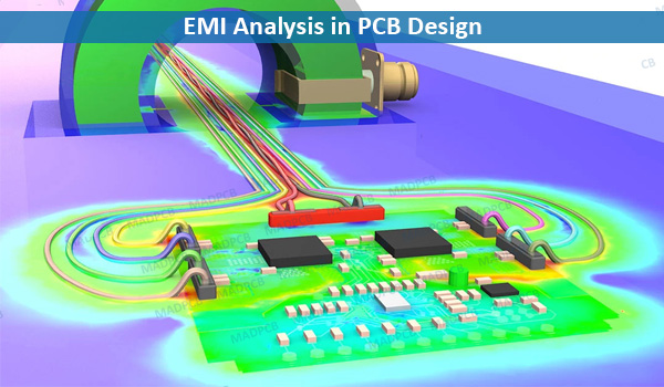
PCB Design Guidelines For EMI EMC - RayMing PCB
 www.raypcb.com
PCB Design Guidelines For EMI EMC - RayMing PCB
Some LVDS PCB Layout Guidelines For Ensuring Signal Integrity | PCB
 resources.altium.com
Some LVDS PCB Layout Guidelines for Ensuring Signal Integrity | PCB ...
Some LVDS PCB Layout Guidelines For Ensuring Signal Integrity | PCB
 resources.altium.com
Some LVDS PCB Layout Guidelines for Ensuring Signal Integrity | PCB ...
Some LVDS PCB Layout Guidelines For Ensuring Signal Integrity | PCB
Some LVDS PCB Layout Guidelines for Ensuring Signal Integrity | PCB ...
PCB Layout Rules For PCIE, SATA, LAN, LVDS, USB, SDVO,
 www.fedevel.com
PCB layout rules for PCIE, SATA, LAN, LVDS, USB, SDVO,
Some lvds pcb layout guidelines for ensuring signal integrity. Pcb layout guidelines top 5 pcb design rules you need to know. pcb design layout guidelines for engineers